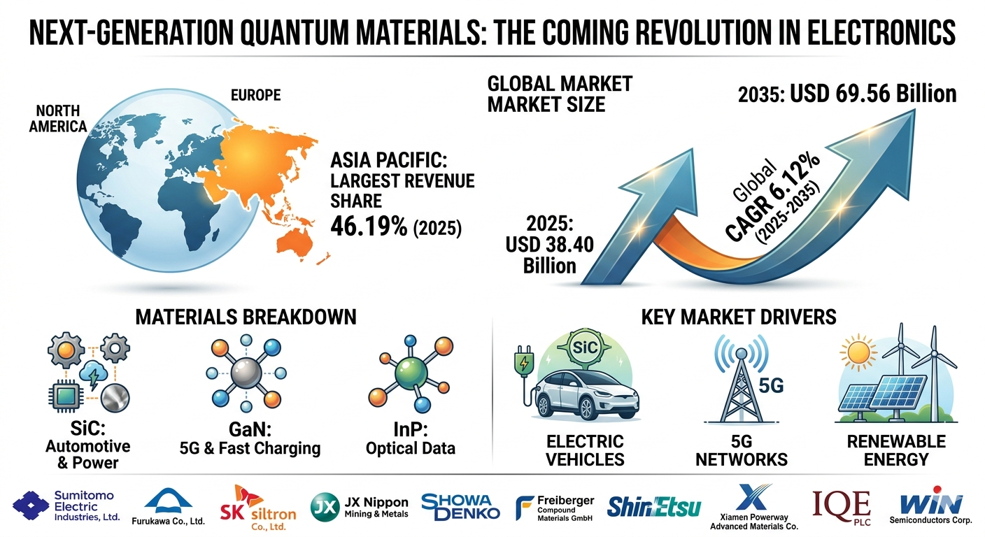
The critical infrastructure underpinning modern telecommunications, high-power electronics, and automotive electrification is shifting toward next-generation chemical architectures. As silicon approaches its physical breakdown limits, compound semiconductors comprising two or more elemental segments from the periodic table—have emerged as the definitive medium for high-frequency, high-temperature operations. The global compound semiconductor materials market size was valued at USD 38.40 billion in 2025 and is estimated to reach around USD 69.56 billion by 2035. This represents a steady Compound Annual Growth Rate (CAGR) of 6.12% during the forecast period. Driven by rigorous data transmission parameters and vehicle electrification mandates, medium-term predictive modeling projects that the market will achieve a milestone value of approximately USD 57.85 billion by the year 2032.
Market Overview
What are Compound Semiconductor Materials?
Compound semiconductor materials are synthesized crystalline structures formed by combining two or more chemical elements, typically from Groups III and V (e.g., Gallium Nitride [GaN], Indium Phosphide [InP]) or Groups IV and IV (e.g., Silicon Carbide [SiC]) of the periodic table. Unlike elemental silicon, these complex engineered substrates feature a wide bandgap, superior electron mobility, and high saturated electron drift velocity. These precise chemical configurations enable devices to process electronic signals at much higher speeds, withstand extreme operational voltages, and perform reliably under thermal conditions that would cause conventional silicon chips to undergo dielectric breakdown.
Market Dynamics
What Are the Key Factors Driving the Market?
The growth of this market is driven by a profound transformation across the consumer, industrial, and energy infrastructure sectors.
-
Renewable Energy Grid Integration: The accelerating transition toward clean energy grids demands highly efficient inverters and converters capable of handling massive high-voltage direct current (HVDC) transmissions with minimal thermal dissipation.
-
High-Frequency Telecommunications: The global rollout of high-capacity wireless infrastructure demands RF microelectronics that can operate efficiently within millimeter-wave bands.
-
Deep Automotive Decarbonization: Automotive manufacturers are rapidly redesigning drivetrain architectures, moving away from legacy silicon insulated-gate bipolar transistors (IGBTs) to capture the higher efficiency and lightweight benefits offered by wide-bandgap materials.
Market Growth and Regional Breakdown
What is the Geographical Growth Profile of the Market?
Geographically, the industrial demand for advanced substrate manufacturing shows a highly concentrated pattern of development. The Asia-Pacific region dominated the compound semiconductor materials market, holding a commanding 46.19% revenue share in 2025. This regional dominance is anchored by massive industrial wafer fabrication ecosystems, rapid urban migration, and dense concentrations of automotive and consumer electronics supply chains across major manufacturing corridors. While Western economies are scaling up domestic packaging capabilities, the integrated foundries and raw substrate production lines within Asia-Pacific ensure it will remain the primary engine of market volume and revenue growth throughout the decade.
Key Market Trends
What are the Primary Technological Shifts Redefining the Market?
The technical evolution of this industry is currently defined by three distinct macro-trends that leverage the unique chemical traits of advanced compound crystals:
Rise of 5G Networks and Millimeter-Wave Infrastructure
The widespread adoption of 5G networks, which prioritize exceptional speeds and ultra-low latency, has vastly increased the performance demands placed on telecommunication base stations. To maintain reliable signal amplification at high frequencies, infrastructure deployments rely heavily on Indium Phosphide (InP) and Gallium Nitride (GaN) substrates. These materials deliver the necessary high-speed electronic properties for mobile transceivers and complex beamforming antenna arrays.
Exponential Growth in Electric Vehicle Adoption
Automotive power electronics are undergoing a profound material shift due to the surging global volumes of electric vehicles. Silicon Carbide (SiC) substrates have become the industry standard for traction inverters and onboard charging systems because they can sustain high temperatures and extreme operational voltages. According to the International Energy Agency, global electric car sales approached 14 million units in 2023, underscoring the massive scaling of automotive-grade SiC wafer manufacturing.
Miniaturization of Advanced Electronic Devices
The relentless market demand for compact, lighter, and highly ergonomic consumer products ranging from multi-sensor wearable medical devices to slim-profile smartphones and smartwatches presents deep engineering challenges. To decrease device footprints while maintaining optimal thermal dissipation and processing efficiency, manufacturers are substituting standard silicon with dense SiC and GaN compound semiconductor matrices, preventing localized thermal throttling.
Strategic Data Presentation
How is Segment Data Quantified for Advanced Analysis?
To allow semiconductor researchers and procurement engineers to easily analyze material flows, key operational vectors are structured into a scannable performance matrix below.
| Material Sector Category | Baseline Revenue Share (2025) | Projected Growth Dynamics (2025–2035) | Primary Systemic Growth Catalyst |
| Asia-Pacific Region | 46.19% Market Share | Leading Volume Corridor | Concentrated foundry capacity; dense consumer electronics supply chains. |
| Silicon Carbide (SiC) | Dominant Power Substrate | High-Voltage Acceleration | Massive transition to 800V EV traction inverters and rapid-charging infrastructure. |
| Gallium Nitride (GaN) | High-Frequency Leader | Rapid Consumer/Telecom Growth | High-density fast chargers, 5G base stations, and RF power amplifiers. |
| Indium Phosphide (InP) | Specialized Opto-Sector | High-Speed Data Center Demand | Laser sources for optical transceivers and high-bandwidth telecom networks. |
| Automotive Application | High-Value Growth Segment | Exponential Integration Vector | Strict driving range requirements and high-temperature operating limits. |
Benefits of Using Compound Semiconductor Materials
What are the Mechanical and Thermal Performance Advantages?
Integrating compound semiconductor materials into high-power electrical circuits yields immediate physical advantages over traditional silicon. Because these materials feature a wide bandgap, they exhibit dielectric breakdown fields that are significantly higher than those of standard silicon. This enables thin wafer substrates to reliably manage high operational voltages.
Furthermore, the superior thermal conductivity of materials like Silicon Carbide (SiC) allows components to dissipate excess heat with exceptional efficiency. This drastically reduces the size and weight of passive cooling blocks and liquid-thermal management loops. Ultimately, this material swap translates to reduced power conversion losses, smaller product footprints, and highly optimized energy efficiency ratings.
Market Recent Government Initiatives
What Legislative Frameworks are Shaping Substrate Supply Chains?
National governments are increasingly treating domestic substrate manufacturing capacity as a matter of critical economic security. In the United States, ongoing funding allocations from the CHIPS and Science Act are targeting the domestic production of wide-bandgap materials, specifically prioritizing military-grade GaN and SiC infrastructure. Similarly, the European Chips Act provides substantial capital subsidies to establish advanced wafer foundries within the EU, aiming to reduce dependence on external supply chains. Across Asia, targeted tax incentives and sovereign technology funds are actively financing the expansion of high-purity crystalline ingot growing facilities to secure long-term market leadership.
Competitive Landscape: Top Companies Profiled
What are the Corporate Portfolios of Major Market Leaders?
Sumitomo Electric Industries, Ltd.
- About: Based in Osaka, Japan, Sumitomo Electric is a world-class manufacturer of electrical wire and optical fiber cables, maintaining an advanced position in the synthesis of compound semiconductor substrates like Gallium Arsenide (GaAs) and Gallium Nitride (GaN).
- Products & Services: High-purity compound semiconductor wafers, optoelectronic devices, electronic materials, and advanced RF components for telecommunications.
- Market Capitalization: Approximately JPY 8.71 trillion / USD 56 billion (Evaluated Q2 2026).
Shin-Etsu Chemical Co., Ltd.
- About: As a global leader in chemical and silicon substrate manufacturing, Tokyo-headquartered Shin-Etsu has expanded its technical portfolio to deliver high-quality GaN-on-Silicon and specialized compound crystal technologies.
- Products & Services: Semiconductor silicon wafers, synthetic quartz, polyvinyl chloride, and next-generation compound epitaxial thin-films.
- Market Capitalization: Approximately JPY 13.53 trillion / USD 83.30 billion (Evaluated Q2 2026).
IQE PLC
- About: Operating out of Cardiff, United Kingdom, IQE is the premier global outsource provider of advanced compound semiconductor wafer products and epitaxy services.
- Products & Services: Advanced epitaxial wafers (GaAs, InP, GaN) utilized in wireless communications, optical communications, and advanced sensor modules.
- Market Capitalization: Approximately GBP 403.22 million / USD 620 million (Evaluated Q2 2026).
Furukawa Co., Ltd.
- About: A historic Japanese industrial group, Furukawa maintains a highly specialized advanced materials division focused on high-purity metals and crystalline compounds required for technical industrial electronics.
- Products & Services: High-purity metallic arsenic, compound semiconductor materials, industrial machinery, and specialized electronic chemicals.
- Market Capitalization: Approximately JPY 3.73 trillion / USD 23.33 billion (Evaluated Group-wide Level, Q2 2026).
Recent Developments by Major Companies
What Strategic Corporate Actions are Altering Market Dynamics?
The competitive landscape is defined by aggressive investments to transition production from legacy 150mm (6-inch) wafers to high-efficiency 200mm (8-inch) crystal architectures. Throughout late 2025 and early 2026, leading entities such as SK siltron and Showa Denko (Resonac) completed major expansions of their manufacturing facilities to secure higher production yields of automotive-grade SiC substrates. Concurrently, specialized epitaxy leaders like IQE PLC signed multi-year supply agreements with major defense and aerospace electronics firms. These partnerships focus on delivering high-reliability GaN-on-Diamond wafers, a technology designed to meet the extreme thermal dissipation needs of next-generation satellite radar networks and advanced artificial intelligence hardware.
Future of the Market
What Long-Term Structural Paradigms Will Define this Sector?
The future of the compound semiconductor materials sector will be characterized by the rise of ultra-wide bandgap (UWBG) architectures that transcend the limits of current technologies. Over the next decade, while GaN and SiC solidify their roles as mainstream industrial materials, research will pivot sharply toward the commercial production of Gallium Oxide ($\text{Ga}_2\text{O}_3$) and synthetic diamond substrates. These advanced crystal materials offer breakdown voltages and thermal coping capacities that are exponentially higher than current standards. Consequently, the industry will evolve into a deeply fragmented, application-specific ecosystem where materials are precisely matched to extreme operational environments—ultimately enabling the deployment of deep-space exploration electronics, sub-surface quantum computing hubs, and ultra-dense hypersonic defense arrays.
Why Is the Market Important?
At its core, this market serves as the foundational material layer that enables the advancement of global computing, decarbonization, and high-speed data communications. Without the scaling of these compound materials, the infrastructure goals of the modern world would hit a definitive performance wall under the thermal constraints of standard silicon. By providing materials capable of operating at extreme energy frequencies and voltages, this industry directly unlocks the real-world performance potential of next-generation EV platforms, high-speed 5G/6G data hubs, and highly efficient clean energy grids. It stands as a vital pillar ensuring the continuity of global technological innovation.
About Us
Towards Chemical and Materials is a leading global consulting firm specializing in providing comprehensive and strategic research solutions across the chemical and materials industries. With a highly skilled and experienced consultant team, we offer a wide range of services designed to empower businesses with valuable insights and actionable recommendations.
Our Trusted Data Partners
Precedence Research | Statifacts | Towards Packaging | Towards Healthcare | Towards Food and Beverages | Towards Chemical and Materials | Towards Consumer Goods | Nova One Advisor |
For Latest Update Follow Us: https://www.linkedin.com/company/towards-chem-and-materials/
USA: +1 804 441 9344
APAC: +61 485 981 310 or +91 87933 22019
Europe: +44 7383 092 044
Leave a Reply